Packaging and testing project for Samsung high-end memory chip completed and commissioned in Xi'an on April 14. Lou Qinjian, Shaanxi governor and non-terminal director of Semiconductor Division of Samsung Electronics attended the project completion ceremony.
Samsung Electronics packaging and testing production line started construction in January 2014. It mainly produces SSDs of 3D vertical flash memory chips. Completion of the project marks Samsung chip plant in Xi'an High-tech Zone became the only overseas production base of manufacturing, packaging and testing of Samsung memory chips.
 J-11 fighters in air exercise
 Beauties dancing on the rings
 Attendants-to-be join Mr. & Miss Campus Contest
 Beijing's toughest anti-smoking law takes effect
 Family lives in cave for about 50 years in SW China
 PLA soldiers operating vehicle-mounted guns in drill
 Blind carpenter in E China's Jiangxi
 China hosts overseas disaster relief exercise for the first time
 20 pairs of twins who will become flight attendants in Sichuan
 Obama is sowing discontent in S.China Sea
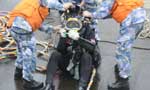 Rescuers work through night to reach cruise ship survivors
 Driving through limbo
 Facing down MERS
Day|Week
 久久精品视频免费试看